Optical Coating & Photolithography
From Volume Production to Precision Custom
From standard functional coatings on glass substrates to precision UV-to-IR optical filters, micron-level photolithographic patterning, and sputtered functional films on resin and 3D parts, we match the right coating process to your specifications and production volume.
Wavelength Range
Down To
Cleanroom
Volume Production
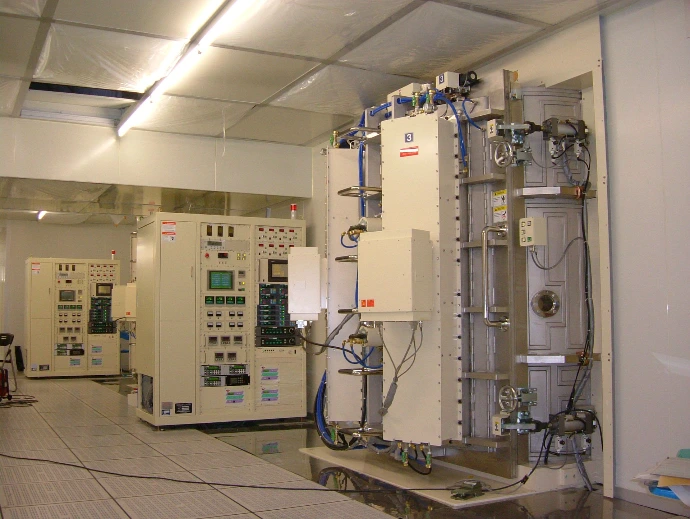
Optical Coating & Photolithography
From Volume Production to Precision Custom
From standard functional coatings on glass substrates to precision UV-to-IR optical filters, micron-level photolithographic patterning, and sputtered functional films on resin and 3D parts, we match the right coating process to your specifications and production volume.
Wavelength Range
Down To
Cleanroom
Volume Production
Choose the Right Coating Solution
Every product has different requirements for specifications, volume, and cost. We offer three coating solutions based on your application, so each project runs on the right process.
Standard Functional Coating
Stable volume production, cost-focused. For glass substrate coatings with defined specifications and high-volume supply needs.
- Anti-reflection (AR) coating
- ITO / FTO transparent conductive film
- Metal sputtering (Cr / Au / Al)
- Dielectric multilayer coating
Precision Optical Coating
Tight optical specifications, from prototype to production. For optical components and sensing applications with strict wavelength, transmittance, and uniformity requirements.
- UV to IR bandpass filters
- Laser mirrors and dichroic mirrors
- Wedge filters and multi-zone filters
- Micron-level photolithographic patterning
Sputtered Functional Films
Low-temperature deposition with strong adhesion. For resin, metal, and 3D-shaped parts that need both function and appearance.
- Aluminum mirrors on resin
- EMI shielding films
- Decorative and color films
- Corrosion-resistant protective layers
Choose the Right Coating Solution
Every product has different requirements for specifications, volume, and cost. We offer three coating solutions based on your application, so each project runs on the right process.
Standard Functional Coating
Stable volume production, cost-focused. For glass substrate coatings with defined specifications and high-volume supply needs.
- Anti-reflection (AR) coating
- ITO / FTO transparent conductive film
- Metal sputtering (Cr / Au / Al)
- Dielectric multilayer coating
Precision Optical Coating
Tight optical specifications, from prototype to production. For optical components and sensing applications with strict wavelength, transmittance, and uniformity requirements.
- UV to IR bandpass filters
- Laser mirrors and dichroic mirrors
- Wedge filters and multi-zone filters
- Micron-level photolithographic patterning
Sputtered Functional Films
Low-temperature deposition with strong adhesion. For resin, metal, and 3D-shaped parts that need both function and appearance.
- Aluminum mirrors on resin
- EMI shielding films
- Decorative and color films
- Corrosion-resistant protective layers
Standard Functional Coating
A range of coating processes for different functional needs, improving the optical and electrical performance of glass substrates.
Anti-Reflection (AR) Coating
Reduces surface reflectance to < 0.5% for higher transmittance. Used in camera lenses, sensor windows, and display cover glass.
ITO / FTO Transparent Conductive Coating
Transparent conductive oxide films with adjustable sheet resistance of 10–200 Ω/□. Used in touch panels, solar cells, and heated defogging glass.
Metal Sputtering (Cr / Au / Al)
Highly adherent metal films for electrode, masking, or heat-dissipation layers. Widely used in MEMS microfabrication and semiconductor wafer processes.
Dielectric Multilayer Coating
Alternating high- and low-index layers for bandpass filters, high reflectors, and beam splitters, with customizable wavelength ranges.
Standard Functional Coating
A range of coating processes for different functional needs, improving the optical and electrical performance of glass substrates.
Anti-Reflection (AR) Coating
Reduces surface reflectance to < 0.5% for higher transmittance. Used in camera lenses, sensor windows, and display cover glass.
ITO / FTO Transparent Conductive Coating
Transparent conductive oxide films with adjustable sheet resistance of 10–200 Ω/□. Used in touch panels, solar cells, and heated defogging glass.
Metal Sputtering (Cr / Au / Al)
Highly adherent metal films for electrode, masking, or heat-dissipation layers. Widely used in MEMS microfabrication and semiconductor wafer processes.
Dielectric Multilayer Coating
Alternating high- and low-index layers for bandpass filters, high reflectors, and beam splitters, with customizable wavelength ranges.
Precision Optical Coating
For high-specification applications in sensors, lasers, semiconductor equipment, and medical instruments, we handle coating design, deposition, and measurement in one flow, with prototypes available from a single piece.
Ion-Assisted Deposition First
Ion-assisted deposition (IAD) is the main process, supported by electron beam evaporation and sputtering. Films are dense, highly adherent, and resistant to moisture-induced spectral shift.
UV to IR Coverage
Covers 250 nm UV to 15 μm IR. Optical simulation and measurement are also available as standalone services.
Wide Range of Substrates
Glass, quartz, resin, metal, and crystal materials; flats, lenses, prisms, and irregular shapes, from small diameters to large substrates.
Full Measurement and Reliability Testing
Managed under an ISO 9001 quality system, with six spectrophotometers, an IR spectrophotometer, laser interferometers, and humidity and thermal shock testing.
Featured Products and Measured Specifications
Steep edges and excellent in-plane uniformity for semiconductor exposure equipment.
| Measured Specifications | |
|---|---|
| Transmittance | Approx. 90% |
| FWHM | ≤ 7 nm |
| Center wavelength variation | ≤ 2 nm (across Φ100 mm) |
A low-UV-absorption deposition method delivers measured curves that match the design with high repeatability.
| Measured Specifications | |
|---|---|
| Transmittance | Approx. 90% (around 220 nm) |
| Reliability | No significant spectral shift after 288 h at 60 °C / 90% RH |
Pass only the absorption band of the target gas. Any center wavelength in the IR range can be designed, with proposals available from a single piece.
| Specifications | |
|---|---|
| Target gases | CH₄, CO₂, CO, NO, SO₂, O₃, SF₆, etc. |
| Applications | NDIR gas sensors and analyzers |
High reflectors for single or multiple laser wavelengths, with selected observation wavelengths transmitted.
| Specifications | |
|---|---|
| KrF 248 nm | Quartz substrate, reflectance ≥ 99.5% |
| YAG and other lasers | Custom for 355 / 532 / 633 / 1,064 nm |
| Multi-laser | Blue, diode, and fiber lasers |
Vary film thickness or combine several coatings on one substrate to simplify optical module design.
| Specifications | |
|---|---|
| Wedge filter | Cut-off wavelength shifts continuously with position |
| Multi-zone filter | Combine ND, AR, dichroic, and metal coatings |
| Applications | Medical diagnostic and office equipment |
Combines anti-reflection and antibacterial performance on glass or resin substrates, with an optional anti-fingerprint (AF) top layer.
| Specifications | |
|---|---|
| Antibacterial effect | Inhibits growth of Staphylococcus aureus and E. coli |
| Applications | Medical optical parts, touch panels |
Infrared Long-Pass Filters (Temperature Sensing and Thermography)
| Specification | Blocking Band (nm) | Blocking Tavg | 5% Cut-On (nm) | 50% Cut-On (nm) | Pass Band (nm) | Pass Tavg |
|---|---|---|---|---|---|---|
| LWP 2.4 μm | 400–2,200 | ≤ 1% | 2,320 ± 30 | 2,400 ± 50 | 2,500–3,600 | ≥ 90% |
| LWP 5.5 μm | 400–5,000 | ≤ 1% | 5,500 ± 400 | — | 7,500–13,500 | ≥ 75% |
| LWP 6.6 μm | 1,500–6,400 | ≤ 1% | 6,600 ± 400 | 6,950 ± 400 | 7,500–14,000 | ≥ 80% |
* Pass-band transmittance above 90% is achievable. 8–14 μm AR coatings and 8–14 μm wideband pass filters are also available for IR cameras, thermography, thermometers, and automotive sensing.
Precision Optical Thin-Film Products
| Category | Products |
|---|---|
| Anti-reflection | Broadband, low-reflection, 3-wavelength, UV-visible, laser, antibacterial, and 8–14 μm IR AR |
| Filters | Bandpass (multi-band, deep UV, IR), IR cut, UV cut, UV-IR cut, ND, ND + IR cut, notch, fluorescence/excitation, and wedge filters |
| Mirrors | Dichroic, cold, hot, laser, and metal (Ag, Al) mirrors |
| Beam splitters | Polarizing beam splitters (PBS), non-polarizing cube beam splitters |
| Functional films | ITO transparent conductive, water-repellent/hydrophilic, anti-fouling, and gas barrier films |
Precision Optical Coating
For high-specification applications in sensors, lasers, semiconductor equipment, and medical instruments, we handle coating design, deposition, and measurement in one flow, with prototypes available from a single piece.
Ion-Assisted Deposition First
Ion-assisted deposition (IAD) is the main process, supported by electron beam evaporation and sputtering. Films are dense, highly adherent, and resistant to moisture-induced spectral shift.
UV to IR Coverage
Covers 250 nm UV to 15 μm IR. Optical simulation and measurement are also available as standalone services.
Wide Range of Substrates
Glass, quartz, resin, metal, and crystal materials; flats, lenses, prisms, and irregular shapes, from small diameters to large substrates.
Full Measurement and Reliability Testing
Managed under an ISO 9001 quality system, with six spectrophotometers, an IR spectrophotometer, laser interferometers, and humidity and thermal shock testing.
Featured Products and Measured Specifications
Steep edges and excellent in-plane uniformity for semiconductor exposure equipment.
| Measured Specifications | |
|---|---|
| Transmittance | Approx. 90% |
| FWHM | ≤ 7 nm |
| Center wavelength variation | ≤ 2 nm (across Φ100 mm) |
A low-UV-absorption deposition method delivers measured curves that match the design with high repeatability.
| Measured Specifications | |
|---|---|
| Transmittance | Approx. 90% (around 220 nm) |
| Reliability | No significant spectral shift after 288 h at 60 °C / 90% RH |
Pass only the absorption band of the target gas. Any center wavelength in the IR range can be designed, with proposals available from a single piece.
| Specifications | |
|---|---|
| Target gases | CH₄, CO₂, CO, NO, SO₂, O₃, SF₆, etc. |
| Applications | NDIR gas sensors and analyzers |
High reflectors for single or multiple laser wavelengths, with selected observation wavelengths transmitted.
| Specifications | |
|---|---|
| KrF 248 nm | Quartz substrate, reflectance ≥ 99.5% |
| YAG and other lasers | Custom for 355 / 532 / 633 / 1,064 nm |
| Multi-laser | Blue, diode, and fiber lasers |
Vary film thickness or combine several coatings on one substrate to simplify optical module design.
| Specifications | |
|---|---|
| Wedge filter | Cut-off wavelength shifts continuously with position |
| Multi-zone filter | Combine ND, AR, dichroic, and metal coatings |
| Applications | Medical diagnostic and office equipment |
Combines anti-reflection and antibacterial performance on glass or resin substrates, with an optional anti-fingerprint (AF) top layer.
| Specifications | |
|---|---|
| Antibacterial effect | Inhibits growth of Staphylococcus aureus and E. coli |
| Applications | Medical optical parts, touch panels |
Infrared Long-Pass Filters (Temperature Sensing and Thermography)
| Specification | Blocking Band (nm) | Blocking Tavg | 5% Cut-On (nm) | 50% Cut-On (nm) | Pass Band (nm) | Pass Tavg |
|---|---|---|---|---|---|---|
| LWP 2.4 μm | 400–2,200 | ≤ 1% | 2,320 ± 30 | 2,400 ± 50 | 2,500–3,600 | ≥ 90% |
| LWP 5.5 μm | 400–5,000 | ≤ 1% | 5,500 ± 400 | — | 7,500–13,500 | ≥ 75% |
| LWP 6.6 μm | 1,500–6,400 | ≤ 1% | 6,600 ± 400 | 6,950 ± 400 | 7,500–14,000 | ≥ 80% |
* Pass-band transmittance above 90% is achievable. 8–14 μm AR coatings and 8–14 μm wideband pass filters are also available for IR cameras, thermography, thermometers, and automotive sensing.
Precision Optical Thin-Film Products
| Category | Products |
|---|---|
| Anti-reflection | Broadband, low-reflection, 3-wavelength, UV-visible, laser, antibacterial, and 8–14 μm IR AR |
| Filters | Bandpass (multi-band, deep UV, IR), IR cut, UV cut, UV-IR cut, ND, ND + IR cut, notch, fluorescence/excitation, and wedge filters |
| Mirrors | Dichroic, cold, hot, laser, and metal (Ag, Al) mirrors |
| Beam splitters | Polarizing beam splitters (PBS), non-polarizing cube beam splitters |
| Functional films | ITO transparent conductive, water-repellent/hydrophilic, anti-fouling, and gas barrier films |
Photolithographic Patterning
By combining photoresist processing with thin-film deposition, different functional coatings can be placed precisely on one substrate for sensors, camera modules, encoders, and optical communication components.
Coating and Patterning in One Flow
Deposition and patterning are completed on the same line using lift-off or etching, reducing handling risk and lead time.
Micron-Level Accuracy
Mask alignment replaces mechanical holders, enabling dichroic line/space patterns down to 1 μm.
Sharp Boundaries, Smaller Gaps
Pattern edge blur of about 5 μm versus about 100 μm with metal masks, so adjacent filter regions such as RGB bandpass filters can sit side by side.
Multi-Function Integration
Combine several coatings on one substrate, such as dichroic + light-shielding or mirror + absorptive + AR, to simplify optical module design.
Patterning Specifications
- Patterning processLift-off / Etching
- Pattern accuracyLine/space down to 1 μm
- ExposureMask aligner
- Max. substrate sizeΦ6 in
- Max. substrate thickness25 mm (prisms supported)
- Dielectric multilayer patterningFilm thickness up to 7 μm
- EnvironmentISO Class 1 cleanroom
* Achievable accuracy depends on coating type and pattern design. Send us your drawings for evaluation.
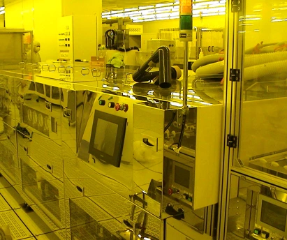
Photolithographic Patterning
By combining photoresist processing with thin-film deposition, different functional coatings can be placed precisely on one substrate for sensors, camera modules, encoders, and optical communication components.
Coating and Patterning in One Flow
Deposition and patterning are completed on the same line using lift-off or etching, reducing handling risk and lead time.
Micron-Level Accuracy
Mask alignment replaces mechanical holders, enabling dichroic line/space patterns down to 1 μm.
Sharp Boundaries, Smaller Gaps
Pattern edge blur of about 5 μm versus about 100 μm with metal masks, so adjacent filter regions such as RGB bandpass filters can sit side by side.
Multi-Function Integration
Combine several coatings on one substrate, such as dichroic + light-shielding or mirror + absorptive + AR, to simplify optical module design.
Patterning Specifications
- Patterning processLift-off / Etching
- Pattern accuracyLine/space down to 1 μm
- ExposureMask aligner
- Max. substrate sizeΦ6 in
- Max. substrate thickness25 mm (prisms supported)
- Dielectric multilayer patterningFilm thickness up to 7 μm
- EnvironmentISO Class 1 cleanroom
* Achievable accuracy depends on coating type and pattern design. Send us your drawings for evaluation.
Sputtered Functional Films
High-speed sputtering causes minimal heat damage, forming uniform, dense, and highly adherent films on resin, metal, and 3D-shaped parts.
No Hard Coat Needed on Resin
With SiO₂ polymerization treatment, aluminum can be coated on acrylic and other resins without a hard coat, with no peeling after dozens of tape tests.
Uniform on Curved Surfaces
Film thickness is nearly identical at the top and bottom of steep lenses, keeping reflectance variation low.
Corrosion-Resistant Protection
Aluminum with a silicon oxide protective layer shows no change after more than 10 minutes under 1% KOH solution, with stable results in volume production.
Interference Colors
Multilayer interference produces a wide range of colors, and custom colors can be discussed.
Sputtering Specifications
- Max. workpiece sizeW160 × L325 × H110 mm
- Resin substratesPC, PET, PBT, ABS, PMMA, COP, COC
- Other substratesGlass, metal, silicon wafers, lenses, 3D parts
- Al mirror reflectance on resinApprox. 89–90% (400–700 nm)
- Batch consistencyNegligible variation across 5 batches
* Max. workpiece size refers to the effective area for Al + SiOx films. Reflectance measured on PC substrates.
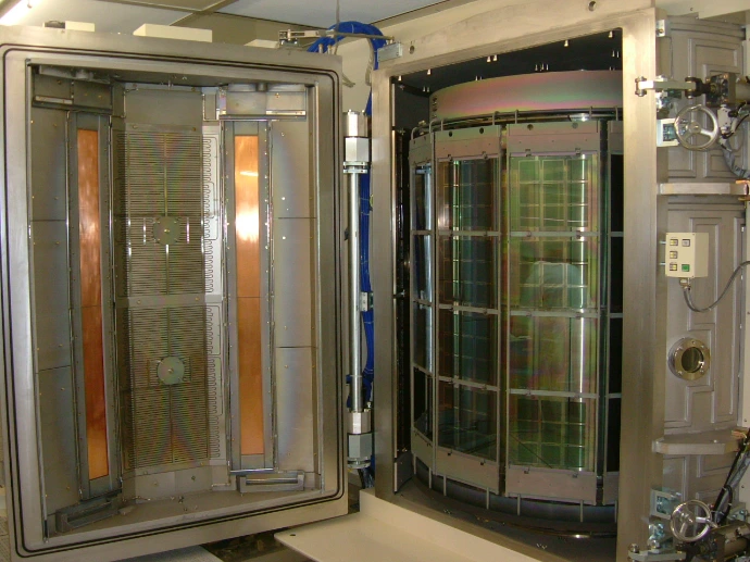
Available Materials
Metal films
Oxide films
EMI Shielding Films
Ag > Cu > Al > Cr > Ti
Shielding performance ranking measured at 50 MHz–1 GHz. Oxide AR coatings provide no shielding.
- AlEffective from 50 nm, better at 500 nm+
- Ag, CuHigh shielding from 100 nm
- CrClear shielding from 500 nm
- TiEffective at 1,000 nm
Application Examples
Sputtered Functional Films
High-speed sputtering causes minimal heat damage, forming uniform, dense, and highly adherent films on resin, metal, and 3D-shaped parts.
No Hard Coat Needed on Resin
With SiO₂ polymerization treatment, aluminum can be coated on acrylic and other resins without a hard coat, with no peeling after dozens of tape tests.
Uniform on Curved Surfaces
Film thickness is nearly identical at the top and bottom of steep lenses, keeping reflectance variation low.
Corrosion-Resistant Protection
Aluminum with a silicon oxide protective layer shows no change after more than 10 minutes under 1% KOH solution, with stable results in volume production.
Interference Colors
Multilayer interference produces a wide range of colors, and custom colors can be discussed.
Sputtering Specifications
- Max. workpiece sizeW160 × L325 × H110 mm
- Resin substratesPC, PET, PBT, ABS, PMMA, COP, COC
- Other substratesGlass, metal, silicon wafers, lenses, 3D parts
- Al mirror reflectance on resinApprox. 89–90% (400–700 nm)
- Batch consistencyNegligible variation across 5 batches
* Max. workpiece size refers to the effective area for Al + SiOx films. Reflectance measured on PC substrates.
Available Materials
Metal films
Oxide films
EMI Shielding Films
Ag > Cu > Al > Cr > Ti
Shielding performance ranking measured at 50 MHz–1 GHz. Oxide AR coatings provide no shielding.
- AlEffective from 50 nm, better at 500 nm+
- Ag, CuHigh shielding from 100 nm
- CrClear shielding from 500 nm
- TiEffective at 1,000 nm
Application Examples
Applications and Additional Services
From medical and measurement to semiconductor and laser equipment, we also handle pre- and post-coating processes to reduce handoffs between suppliers.
Applications
Additional Services
Precision cleaning, glass dicing, polishing, edge blackening, assembly and bonding, plus inspection and measurement services. We handle everything from single prototypes to volume production, and common bandpass filters are in stock as single pieces for development testing.
Applications and Additional Services
From medical and measurement to semiconductor and laser equipment, we also handle pre- and post-coating processes to reduce handoffs between suppliers.
Applications
Additional Services
Precision cleaning, glass dicing, polishing, edge blackening, assembly and bonding, plus inspection and measurement services. We handle everything from single prototypes to volume production, and common bandpass filters are in stock as single pieces for development testing.
What to Include in Your Inquiry
Coating quotes depend on the substrate, coating type, and specifications. Sharing the details below in your first inquiry helps us assess feasibility faster and give you an accurate quote and lead time.
Application
What the part is used for, such as sensors, camera modules, laser equipment, displays, or medical instruments.
Substrate
Material (glass, quartz, resin, silicon wafer, metal, etc.), form (flat, lens, prism, 3D part), dimensions, and thickness.
Coating Type and Optical Specs
Coating type (AR, bandpass, mirror, ITO, metal, etc.), wavelength range, target transmittance or reflectance, and angle of incidence. Please attach spectral curves if available.
Coated Surfaces and Patterns
Single- or double-sided coating. For photolithographic patterning or partial coating, please attach a drawing with pattern dimensions and tolerances.
Reliability Requirements
Operating environment and test conditions, such as high temperature and humidity, thermal shock, adhesion, or abrasion resistance.
Quantity
Prototype quantity and estimated production volume or annual usage.
Project Stage and Timeline
Whether the project is in development, prototyping, or production, and your target delivery date.
Substrate Supply and Inspection
Whether you will supply the substrates or need us to source them, and whether you need inspection data such as spectral measurements.
What to Include in Your Inquiry
Coating quotes depend on the substrate, coating type, and specifications. Sharing the details below in your first inquiry helps us assess feasibility faster and give you an accurate quote and lead time.
Application
What the part is used for, such as sensors, camera modules, laser equipment, displays, or medical instruments.
Substrate
Material (glass, quartz, resin, silicon wafer, metal, etc.), form (flat, lens, prism, 3D part), dimensions, and thickness.
Coating Type and Optical Specs
Coating type (AR, bandpass, mirror, ITO, metal, etc.), wavelength range, target transmittance or reflectance, and angle of incidence. Please attach spectral curves if available.
Coated Surfaces and Patterns
Single- or double-sided coating. For photolithographic patterning or partial coating, please attach a drawing with pattern dimensions and tolerances.
Reliability Requirements
Operating environment and test conditions, such as high temperature and humidity, thermal shock, adhesion, or abrasion resistance.
Quantity
Prototype quantity and estimated production volume or annual usage.
Project Stage and Timeline
Whether the project is in development, prototyping, or production, and your target delivery date.
Substrate Supply and Inspection
Whether you will supply the substrates or need us to source them, and whether you need inspection data such as spectral measurements.
Ready to Get Started?
Send us your specifications or drawings. We will reply within one business day to help you evaluate the right coating process and provide a quote.
Contact UsReady to Get Started?
Send us your specifications or drawings. We will reply within one business day to help you evaluate the right coating process and provide a quote.
Contact Us